Introduction
I will present here a small report on my efforts to remove the RX filters from a TI calypso based phone. The illustrations here are for a Motorola C123, but the same would apply to a lot of other calypso phones since most of them are based around the same reference design.
First off, why would you want to remove those filters ?
Well, they get in the way when you want to receive the uplink frequencies of the GSM band, attenuating the signal by around 30dB. The two main applications where it's useful to receive those are :
- Using the phone as a passive listener ("sniffer")
- Using the phone as a base station ("BTS")
This step is just the "preparation" of your phone hardware for those applications. A lot of further work is needed to actually use the phone like that (if it's even possible), but this is outside the scope of this document.
Preparation
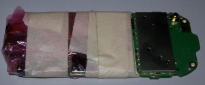
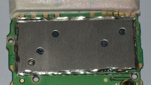
Before getting to the filters removal and replacement, we first need to get access to them. Unfortunately, on the C123, that means getting through the soldered RF shield. Some other calypso phone have a clip-on shield which is easier to remove but those are harder to get a hold of. For more informations on the various models, you can always refer to the "Supported Phone Hardware" list on the OsmocomBB project homepage: here.
If you've already taken appart the phone and shield, just can just skip this section entirely.
Removing the filters
The theory
It's possible to find on the net some reference schematics for the C118/123 phones (and others as well). The reception path always pretty much looks the same and the part we're concerned about looks like the following :
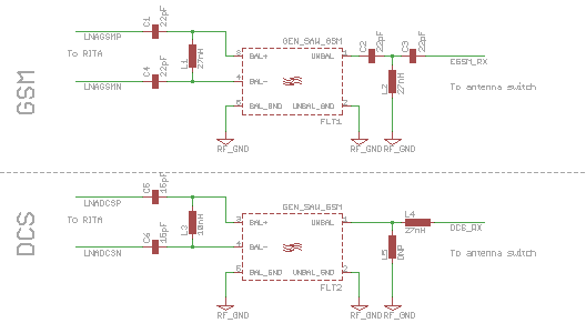
It's divided into the low frequency (GSM900/GSM850) path and high frequency (DCS1800/PCS1900) path. Both are very similar except for little variations on the SAW input matching. As you can see, the filter does more than just filters the signal, it also converts the unbalanced 50 ohm input from the antenna itself to a 100 ohm balanced signal going to the RITA chipset. This means that for a proper modification, we can't just remove the filter and bridge it.
The proper solution is to replace the filter by another component that does the unbalanced to balanced conversion only : a balun. Hopefully, I managed to found some that have almost the same pinout and size as the original filters: TDK HHM1523C1 (for EGSM band) and HHM1526 (for DCS band). The pinout difference lies in the input pin. The original filters have one vertically centered input pin while the baluns have two pins on the upper and lower border. The first one is the input and the second is not connected. This isn't much of a problem because the balun pins are small enough that if you solder the balun in place of the filter, the input and NC pins will not touch the input solder pad. It's then possible to connect the input properly where it needs to be using a small capacitor acting as a RF bridge.
The remaining problem, that I overlooked on my first try, is that what's actually implemented on the phone doesn't match the schematics. It's more like this :
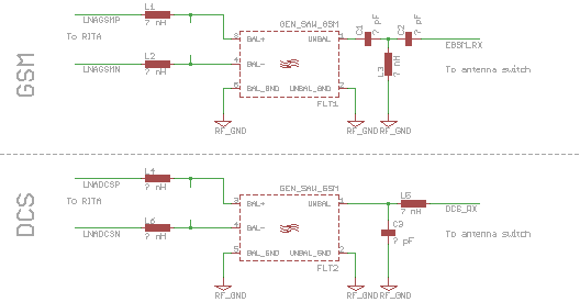
The input matching changes don't matter much. But the connection to the RITA are relevant. Since there is no capacitors in reality, there is no DC isolation between the filter and the RITA. It might not matter for the SAW filter, but for our balun, it's a problem. The RITA outputs are DC-biased to some internal voltage, but the balun is gonna be biased to GND. To make this work, we need to make sure the balun has proper DC blocking on both input and output. For the input, it's already handled because we use a capacitor to connect the input pin as mentionned before. For the output, we need to remove the inductances and replace them by some capacitors of our own.
Pre-requisites
- A hot-air rework station
The filters and replacement baluns are leadless, so no hope to solder/desolder those without hot air. - Fine-tip soldering iron & various smd soldering accessories
Tweezers, magnifying lenses, ... whatever you usually use for that kind of precise work. - HHM1523C1 and HHM1526 baluns
The good news is that Mouser and Digikey stock those and you can buy them in small quantity easily. - 15 pF & 22 pF 0402 high quality capacitors
I didn't have those exact values, so I used 10 pF (for the DCS path) and 20 pF (for the EGSM path). Exact value doesn't matter that much I think. - Patience :)
The 'right way' with baluns
|
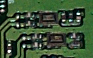
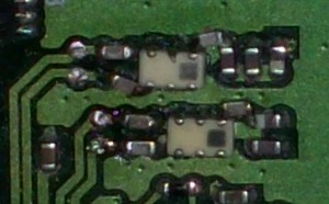
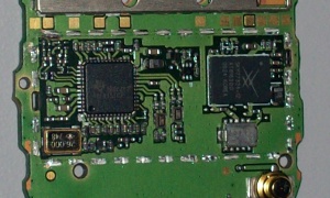
On the right you can see a closeup of the work zone. On the top is the low frequency path and on the bottom, the high frequency one. The first step is to remove the filters and the 0402 inductors at the output. So just use your hot air rework station to heat up the area and pick each component one by one with small tweezers. |
|
|
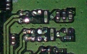
Once the components removed, you can try to clean up the pads using desoldering braid. It's however a very delicate operation because you might end up damaging the pads and/or the traces. You can see on the right that I ripped out two pads and the small traces joining them (on the low frequency path, the pads joining inductor output to filter input). If you do rip some stuff, don't panic and just try to figure some way to deal with it (see below). |
|
|
To put the components back, just apply a very small amount of solder paste to each pads except the filters input pads (the vertically centered ones). Drop the baluns and capacitors on their respective spot and then just heat until reflow. At this point you can inspect visually and electrically for proper contacts. Note that the balun will appear to short both input to the ground, it's normal. So you will have to rely on visual inspection only for the output pads. But you can check that both ground pins are well soldered to the ground and that the NC and input pin are indeed unconnected for now. The final step is to solder the input capacitor on the side for the input. For this just use small amount of solder paste to 'stick' the capacitor in place and heat up with a fine solder iron tip. Note that it's way easier to do if you put the PCB vertically on its side, so that gravity helps you keep the capacitor in place during the work. The final result should look like the picture on the right. As you can see, I had to recover from my damaged pads by putting one of the output capacitor a little weirdly, but it all worked out. |
|
The 'hacked up' way with just caps
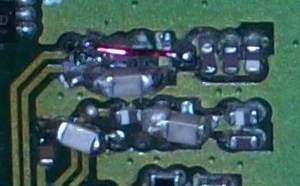
When attempting this for the first try, I soldered / desoldered components a few times and ended up destroying the pads and traces so much that there was no way I could put the original filters or balun back on the PCB.
So in a last attempt to make the phone do something, I tried something a little unorthodox (actually proposed by h0rizon on IRC :). Instead of doing a proper unbalanced to balanced signal convesion, I just connected one of the RITA balanced line to the ground using a DC blocking cap. And then connected the other balanced line to the input via a capacitor as well. For DCS1800 you need to add a capacitor of your own, but for EGSM, there is a capacitor in the input SAW matching that does the trick so you only need a wire.
The quite dirty results is shown on the side. It's ugly but it actually works ... The signal is maybe distorded or a litte more noisy, that has yet to be determined. So if you screw up, you can always fall back to this :)


 Maintained by Sylvain Munaut tnt >at< 246tNt >dot< com